
Printed circuit boards serve as the foundation of nearly every electronic device, providing the electrical pathways that connect components and enable functionality. Before components such as resistors, capacitors, and integrated circuits are assembled onto a board, the circuit board exists in its most basic form. This stage is known as the Bare PCB. Although it may appear simple compared to a fully assembled board, a bare PCB is one of the most critical elements in electronics manufacturing because its quality directly impacts the performance and reliability of the final product.
From consumer electronics and automotive systems to industrial equipment and medical devices, bare PCBs are used across virtually every industry that relies on electronic technology. Understanding what a bare PCB is, how it is manufactured, and why it is important can help businesses make informed decisions when sourcing circuit boards.
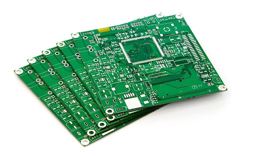
What Is a Bare PCB?
A Bare PCB is a printed circuit board that has completed the fabrication process but does not yet contain any mounted electronic components. It consists only of the substrate material, copper traces, pads, vias, solder mask, and silkscreen markings.
At this stage, the board contains all the required electrical pathways that will later connect electronic components during the assembly process. Because no components are installed, the board is referred to as “bare.”
Bare PCBs are supplied to electronics manufacturers, contract assemblers, and OEMs who then populate the boards with components using SMT (Surface Mount Technology) or through-hole assembly processes.
The quality and accuracy of the bare PCB play a significant role in determining the reliability and performance of the final electronic product.
Structure of a Bare PCB
The structure of a Bare PCB consists of several layers and materials that work together to provide electrical connectivity and mechanical support.
The base material, often called the substrate, forms the core of the board. FR4 fiberglass is the most commonly used substrate due to its excellent balance of cost, strength, and electrical properties. Other materials such as aluminum, Rogers, ceramic, and polyimide may be used for specialized applications.
Copper layers are laminated onto the substrate and etched to create the conductive traces that carry electrical signals and power throughout the board.
A solder mask is applied over the copper traces to protect them from oxidation, contamination, and accidental short circuits. The solder mask also helps improve the appearance of the board.
Silkscreen markings are added to identify component locations, reference designators, logos, and manufacturing information.
The completed board contains all required circuitry and features but remains free of electronic components until assembly.
Manufacturing Process of a Bare PCB
The production of a Bare PCB involves multiple precision manufacturing steps designed to create accurate and reliable circuit patterns.
The process begins with selecting the appropriate substrate material based on the application requirements. Copper-clad laminates are prepared and cleaned to ensure proper adhesion.
A photoresist layer is applied to the copper surface, and the circuit design is transferred using ultraviolet light exposure. The exposed board is then developed to reveal the circuit pattern.
The unwanted copper is removed through chemical etching, leaving only the desired traces and pads.
Drilling is performed to create holes for vias and through-hole components. These holes are then plated with copper to establish electrical connections between layers.
For multilayer boards, individual layers are laminated together under controlled pressure and temperature conditions.
A solder mask is applied to protect the circuitry, followed by silkscreen printing for identification purposes.
Finally, the bare PCB undergoes electrical testing and inspection to verify that all circuits function correctly before shipment.
Importance of Bare PCB Quality
The quality of a Bare PCB is essential because defects at this stage can lead to assembly issues, product failures, and increased manufacturing costs.
Accurate trace widths and spacing are necessary to ensure proper electrical performance and signal integrity. Poorly fabricated traces can result in short circuits, open circuits, or inconsistent operation.
Hole accuracy is equally important, particularly in multilayer boards where vias connect different layers. Misaligned or improperly plated holes can compromise reliability.
Surface finish quality also plays a critical role in component assembly. A high-quality finish ensures proper solderability and long-term durability.
By maintaining strict quality standards during fabrication, manufacturers can minimize defects and improve overall product performance.
Advantages of Bare PCBs
One of the primary advantages of a Bare PCB is that it allows manufacturers to verify circuit board quality before investing in component assembly. Testing the bare board helps identify fabrication issues early in the production process.
Bare PCBs also provide flexibility in assembly operations. The same board design can be used for multiple product variants by populating different components.
Another advantage is cost efficiency. Purchasing bare PCBs separately allows manufacturers to manage inventory and production schedules more effectively.
The fabrication process can also be optimized independently from assembly, enabling greater control over quality and lead times.
Additionally, bare PCBs are available in a wide range of materials, layer counts, and configurations to meet diverse application requirements.
Applications of Bare PCBs
The use of Bare PCB technology extends across virtually every electronics industry.
Consumer electronics manufacturers use bare PCBs as the foundation for smartphones, tablets, laptops, gaming systems, and smart home devices.
Automotive companies rely on bare PCBs for engine control modules, infotainment systems, sensors, and electric vehicle electronics.
Industrial automation systems use bare PCBs in controllers, robotics, monitoring equipment, and power management devices.
Medical device manufacturers incorporate bare PCBs into diagnostic equipment, imaging systems, and patient monitoring devices.
Telecommunications infrastructure such as routers, switches, servers, and wireless communication systems also depends on high-quality bare PCBs.
Aerospace and defense applications require precision-fabricated bare PCBs capable of operating in extreme environmental conditions.
Bare PCB Testing and Inspection
Before shipment, every Bare PCB should undergo comprehensive testing and inspection to ensure quality and functionality.
Electrical testing verifies that all intended connections are present and that no unintended short circuits exist. This is often performed using flying probe testing or bed-of-nails testing systems.
Automated optical inspection (AOI) is used to identify defects such as missing traces, incorrect spacing, and manufacturing errors.
Additional inspections may include dimensional measurements, hole verification, and surface finish evaluation.
These quality assurance procedures help ensure that the bare PCB meets design specifications and customer requirements.
Future Trends in Bare PCB Manufacturing
As electronic products continue to evolve, Bare PCB manufacturing is becoming increasingly advanced. Higher layer counts, smaller feature sizes, and more complex designs are driving innovation in fabrication technology.
High-density interconnect (HDI) boards, advanced materials, and laser-drilled microvias are becoming more common as manufacturers seek to support miniaturized and high-performance devices.
Sustainability is also gaining importance, with PCB manufacturers adopting environmentally friendly materials and production methods.
These developments are helping the industry meet the growing demands of emerging technologies such as 5G, artificial intelligence, electric vehicles, and the Internet of Things.
Conclusion
The Bare PCB serves as the foundation of every electronic assembly, providing the essential circuitry that enables electronic devices to function. Its quality, precision, and reliability directly influence the performance of the final product, making PCB fabrication one of the most critical stages in electronics manufacturing.
As technology continues to advance and electronic systems become more complex, the demand for high-quality bare PCBs will continue to grow. Businesses looking for dependable fabrication services often choose an experienced Bare PCB manufacturer to ensure consistent quality, precise manufacturing, and reliable performance for their electronic products.